1 / 5
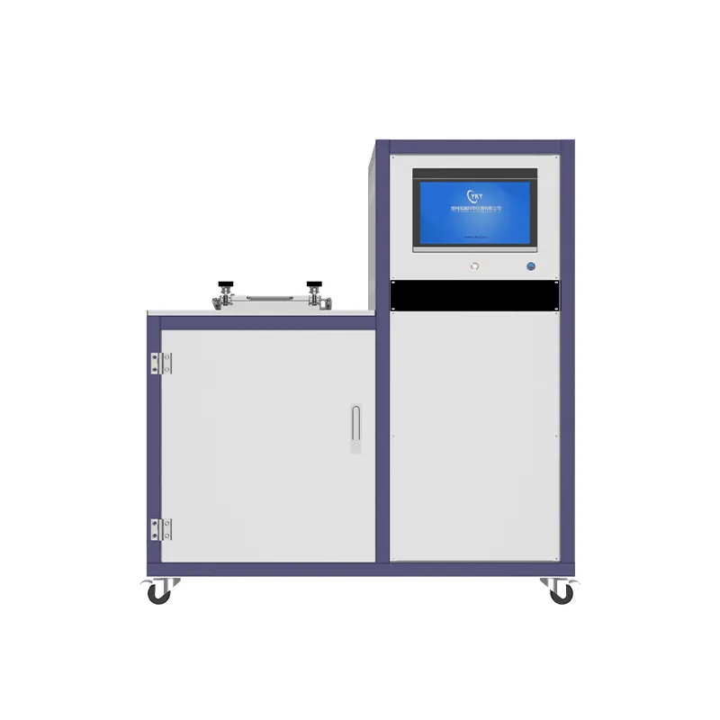
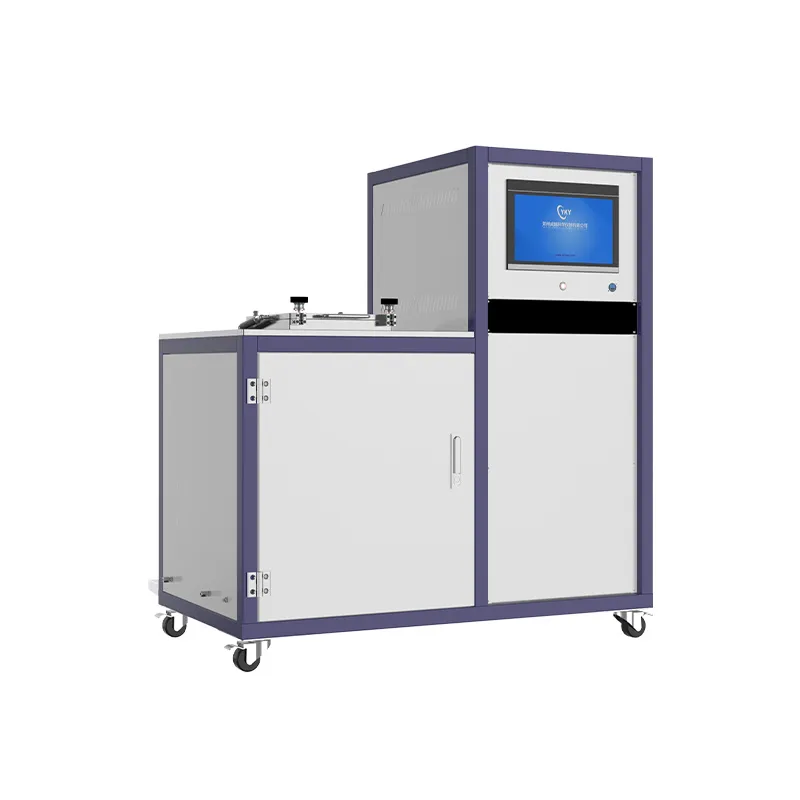
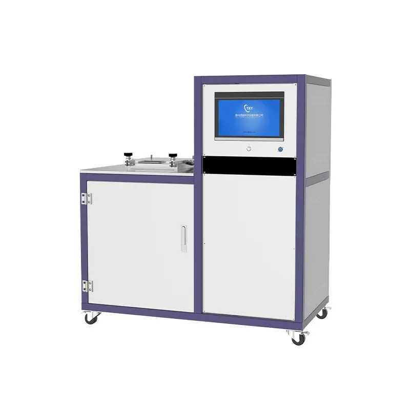
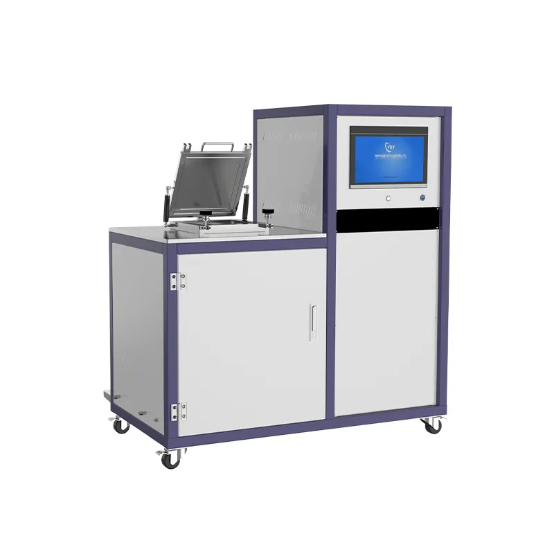
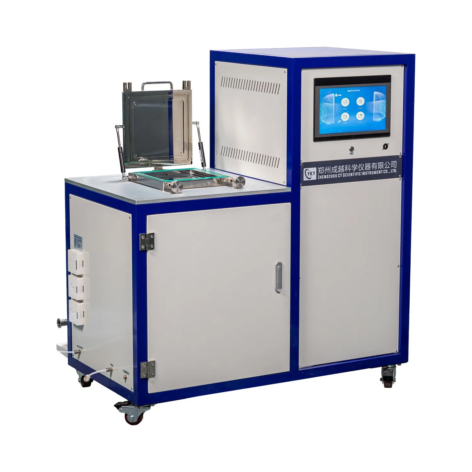
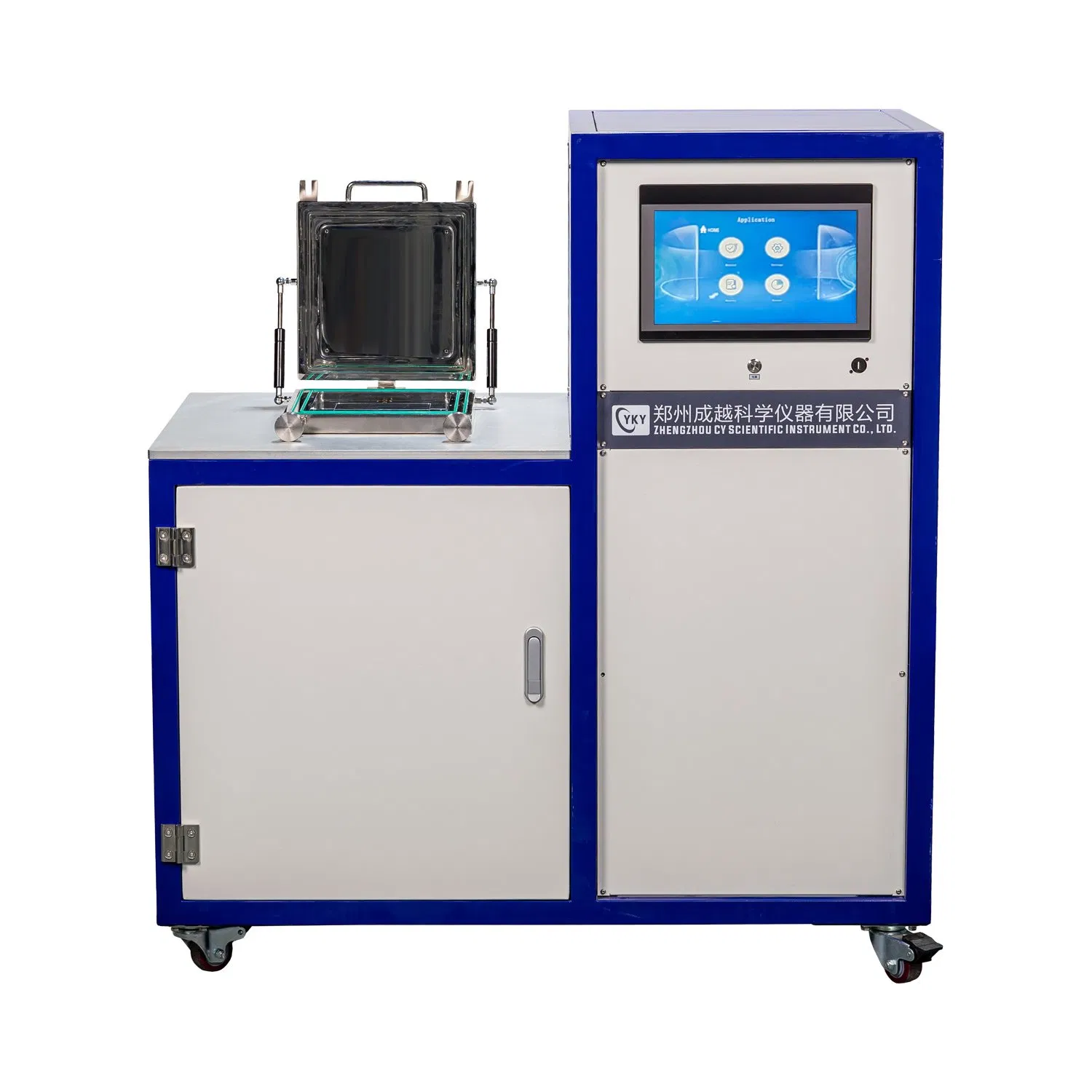
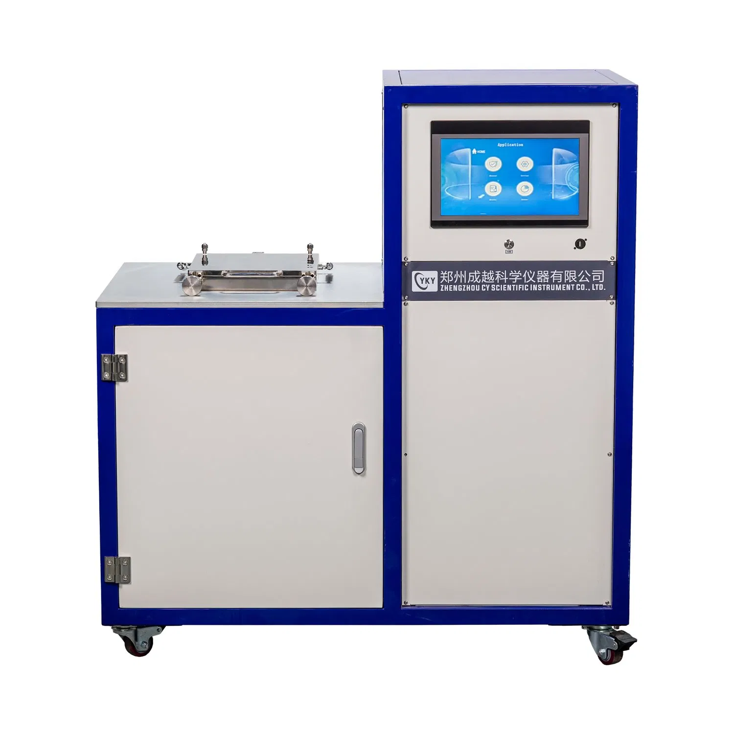
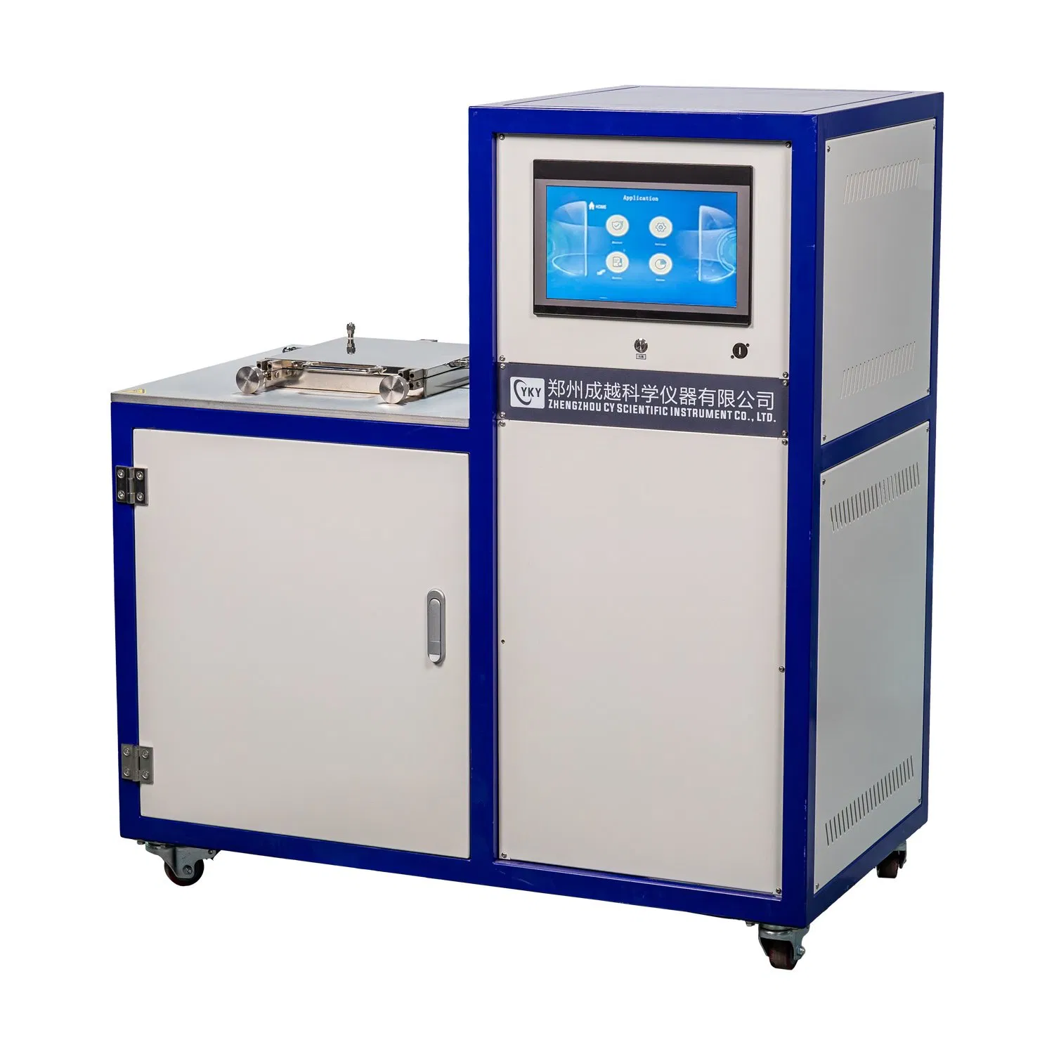
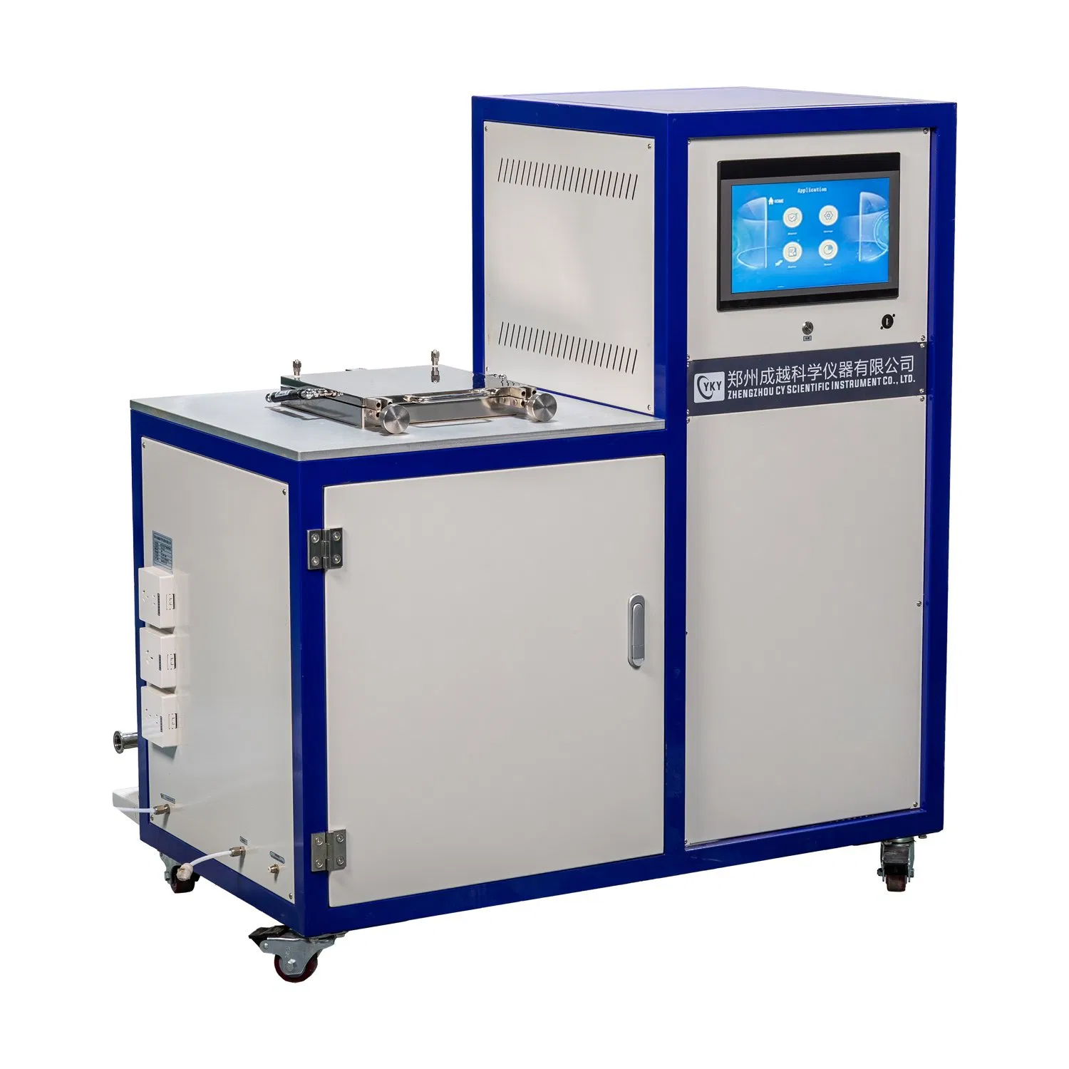
Thermal Atomic Layer Deposition System
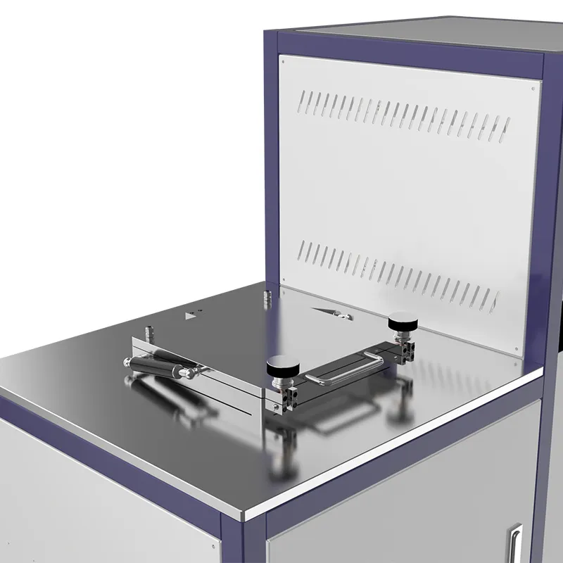
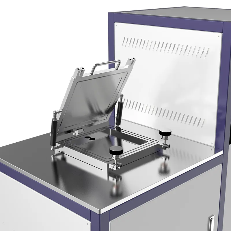
This single-wafer deposition system is specially designed for scientific research and small-scale industrial experiments. Fully compliant with CE standards, it is widely utilized in micro-electronics, nano-materials, optical films, and solar battery technology.
💡 Key Benefits:
Advanced software control system integrating technological formulation, parameter settings, popedom settings, interlocking alarms, and state supervisory control.
Elementary Substances: Co, Cu, Ta, Ti, W, Ge, Pt, Ru, Ni, Fe...
Nitrides: TiN, SiN, AlN, TaN, ZrN, HfN, WN...
Oxides: TiO₂, HfO₂, SiO₂, ZnO, ZrO₂, Al₂O₃, La₂O₃, SnO₂...
Others: GaAs, AlP, InP, GaP, InAs, LaHfxOy, SrTiO₃, SrTaO₆...
| Wafer Dimension | 8 inch and below |
| Wafer Temperature | RT-400ºC, Precision ±0.1ºC |
| Precursor Lines | 3 Lines (Optional expansion) |
| Source Bottle Temp | RT-200ºC, Precision ±0.1ºC |
| Background Vacuum | <5*10⁻³ Torr |
| Growing Mode | Consecutive or Interval |
| Power Supply | 220V/20A AC, 50-60Hz |
| Heterogeneity | < ±1% |
| Instrument Dimension | 600mm x 600mm x 1100mm |